PCB Design and Etching
June 1, 2013
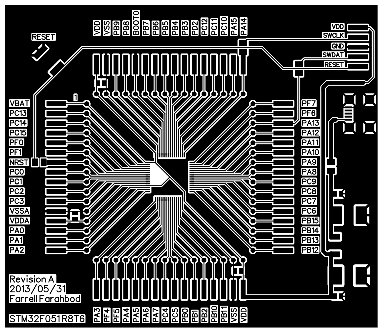
I recently designed a breakout board for the STM32F0. The official STM board is great (and cheap) but I wanted a single-sided board. My laptop has a metal case, and it's tempting to rest a PCB on it sometimes. I'd hate to short out the pin headers.
The end result:
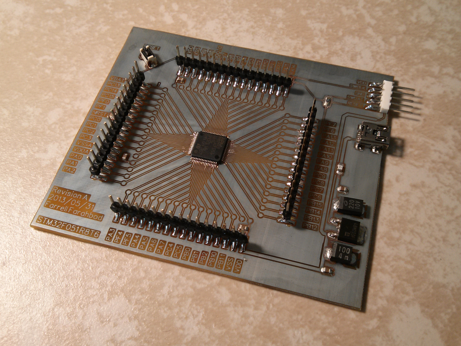
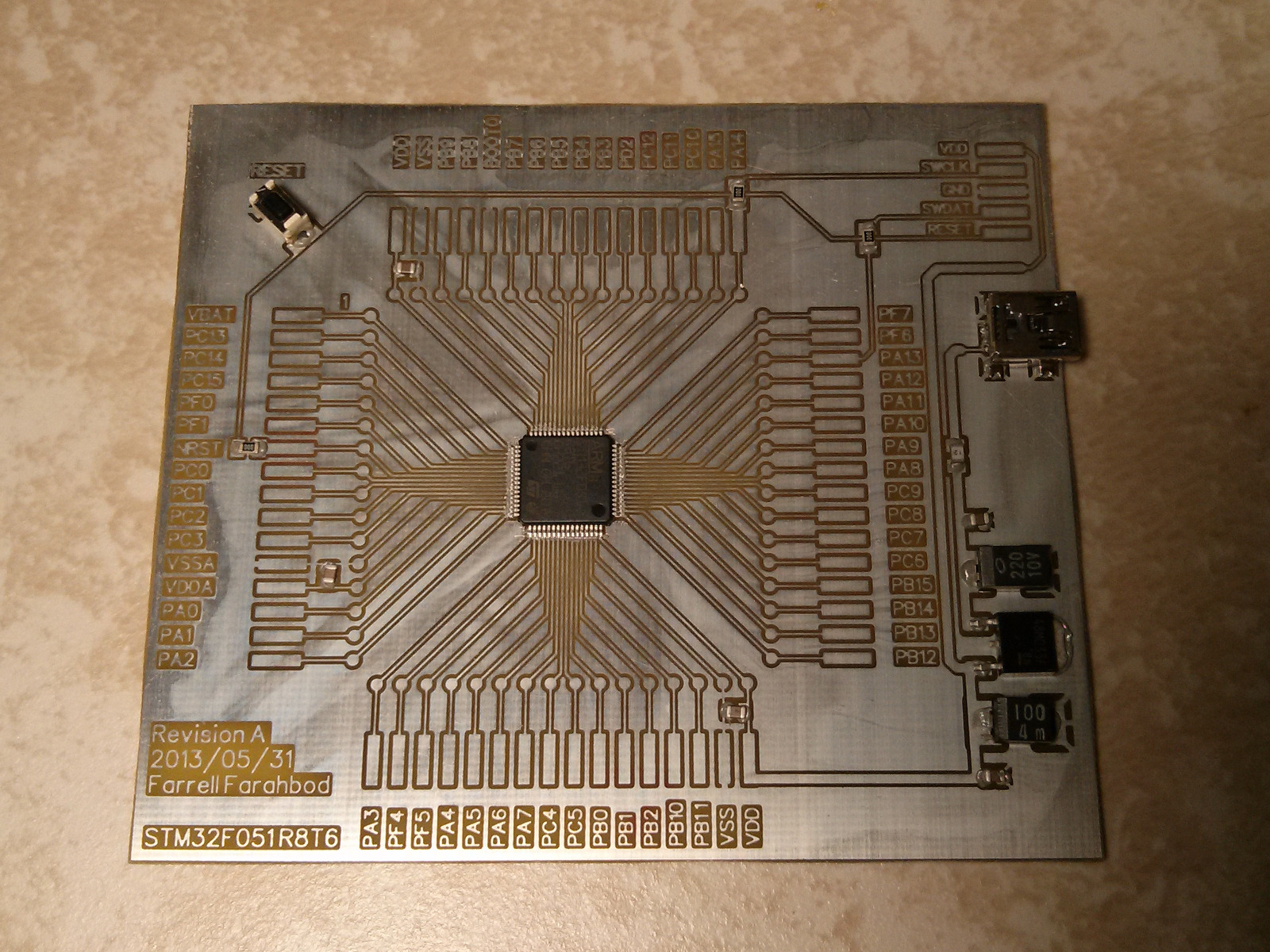
The board is simple: an F0, pin headers for every pin, test points for every pin, a reset button, and a USB port with an LDO regulator to provide 3.3V. I couldn't find surface mount headers locally, so I made some through-hole ones work.
Step 1: Layout the PCB with gEDA.
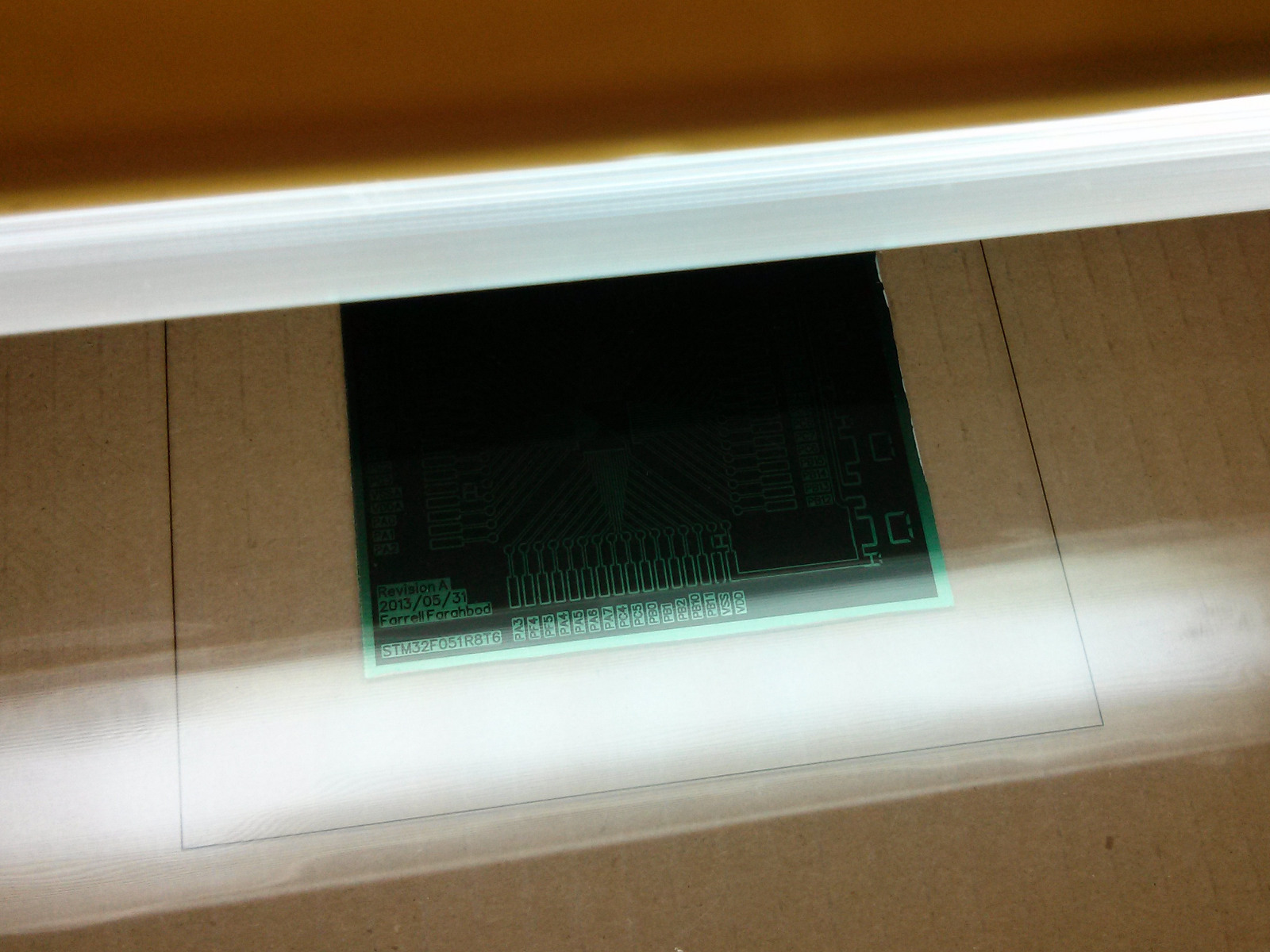
Step 2: Print the design to a transparency, cut a board to size, and expose it with a UV lamp.
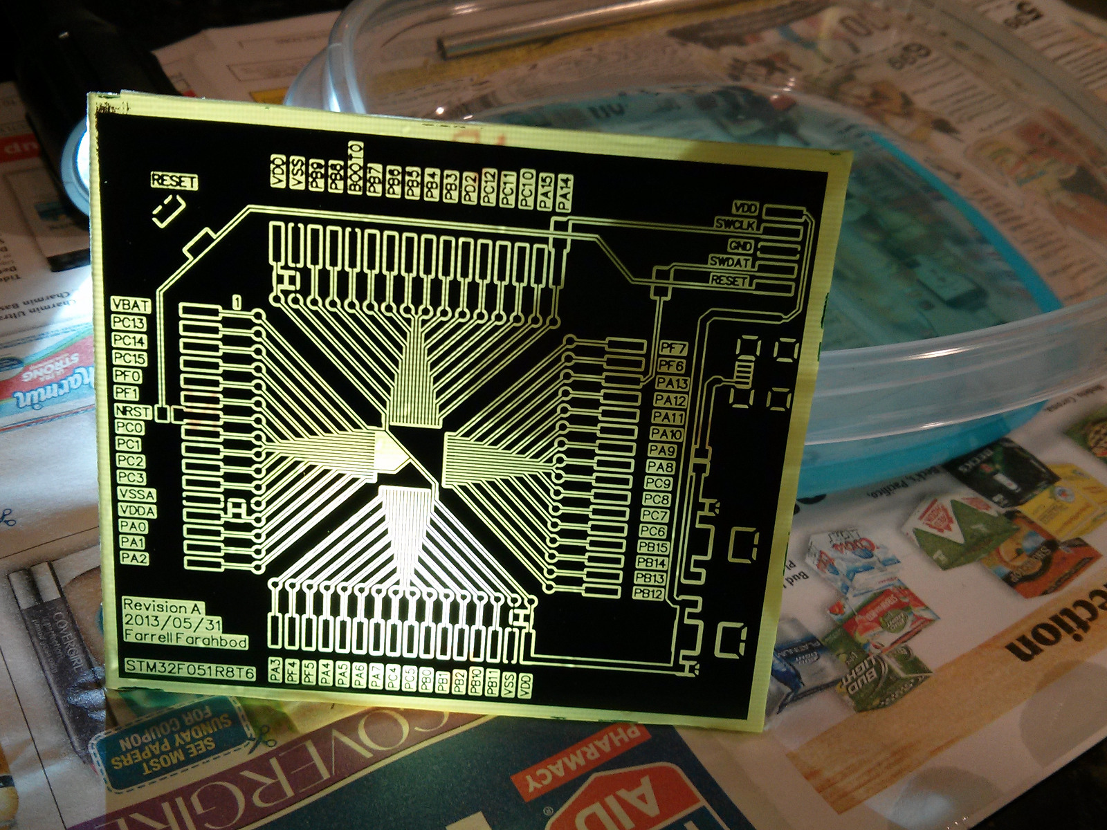
Step 3: Develop the board, then rinse it off.
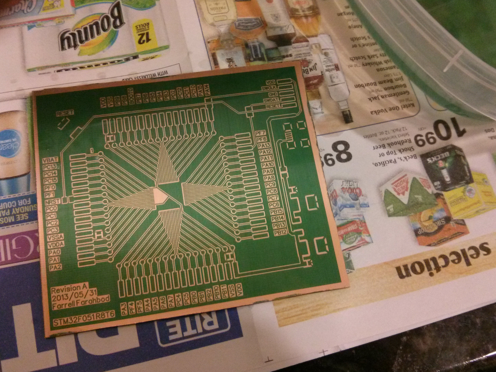
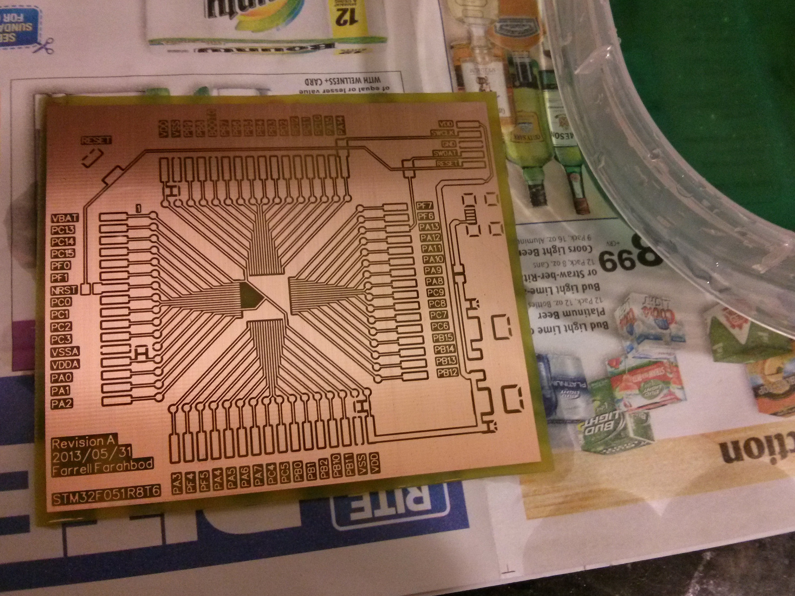
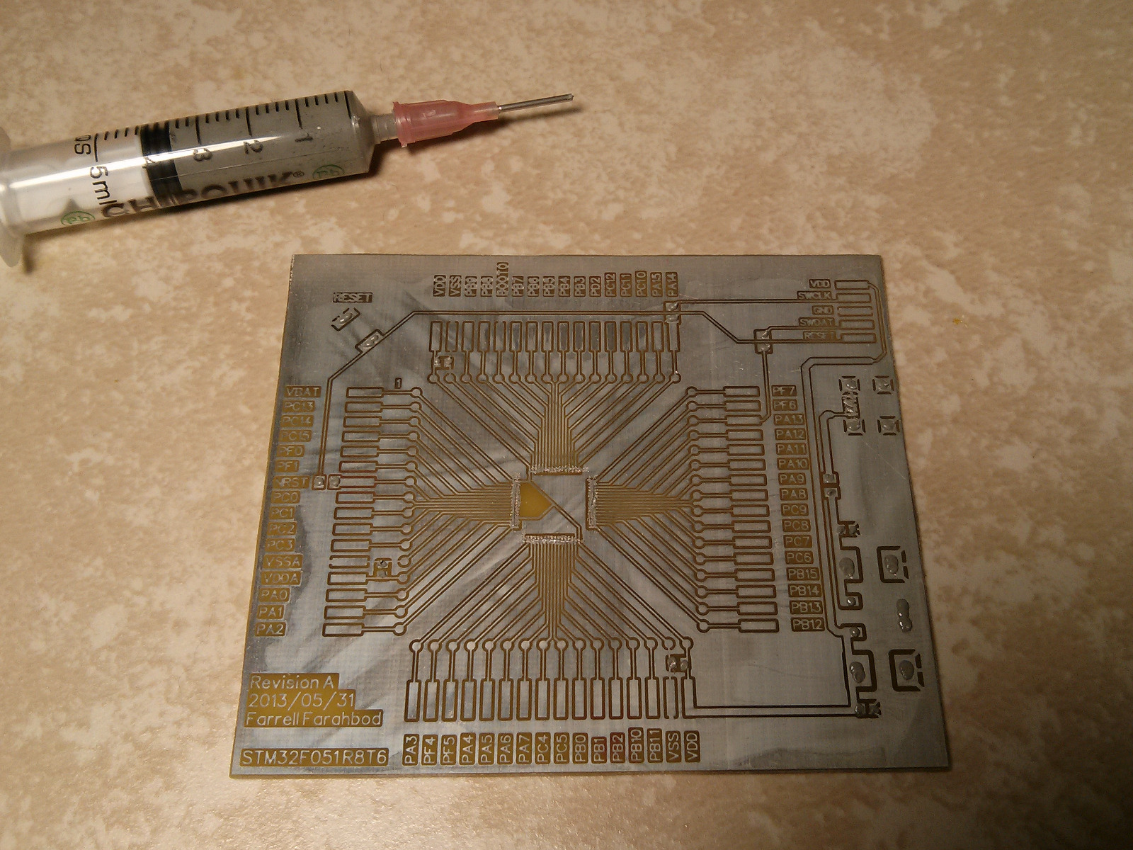
Step 4: Etch the board. I used sodium persulfate for this project.
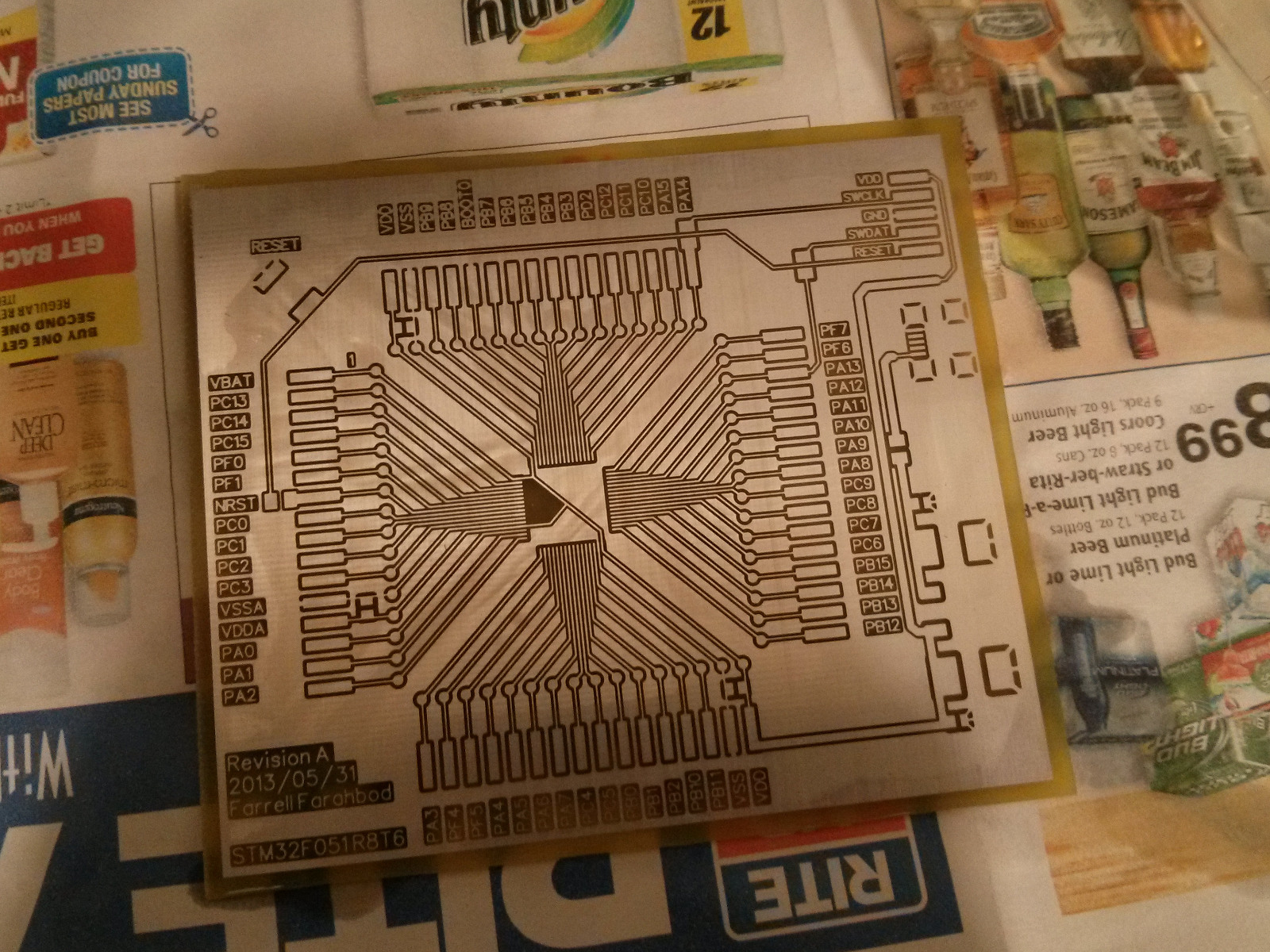
Step 5: Remove the remaining mask by placing the board back into the developer.
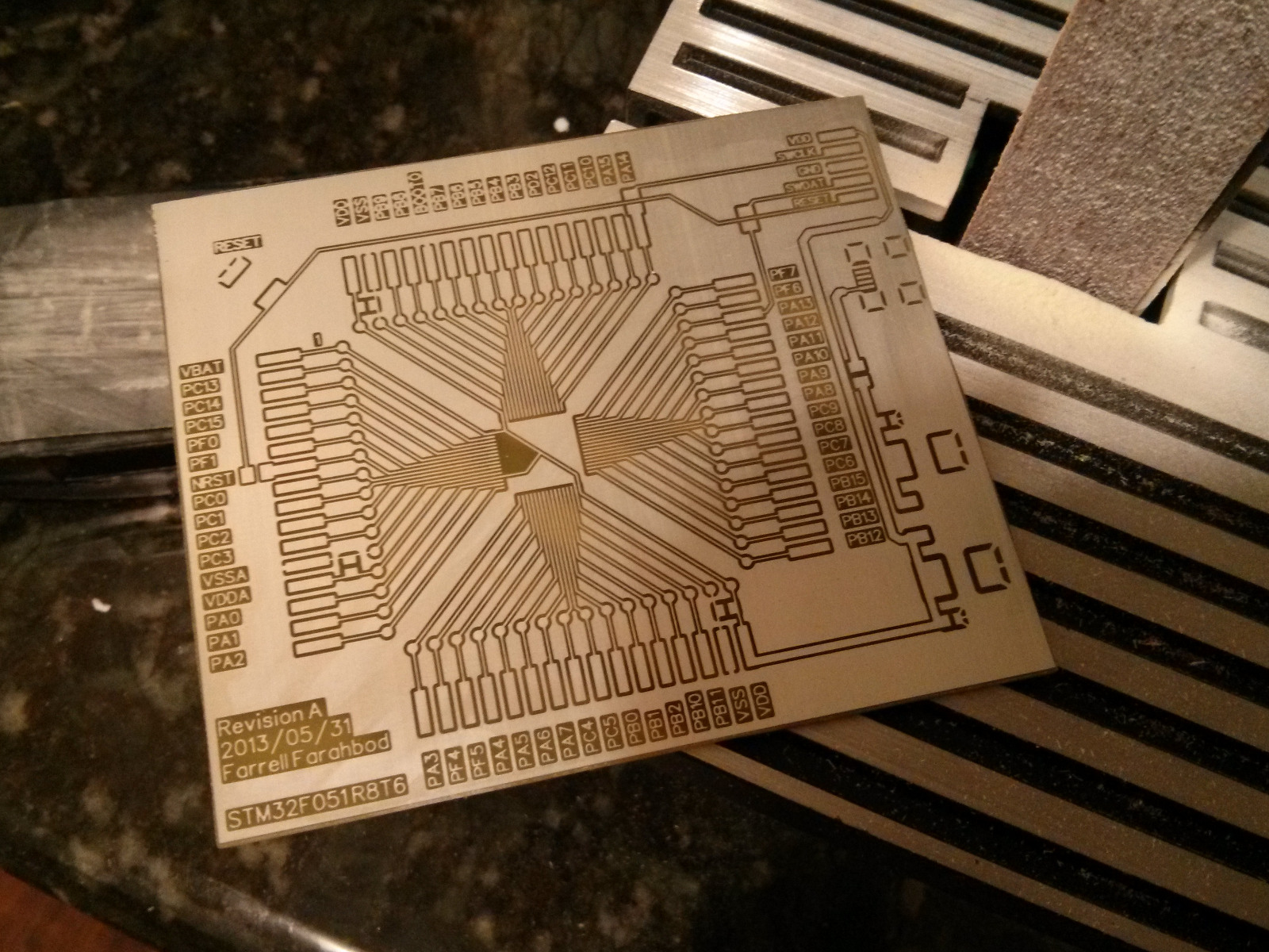
Step 6: Tin plate the board.
Step 7: Sand the board to clean up the edges.
Step 8: Apply solder paste for the SMDs.
Step 9: Place the SMDs.
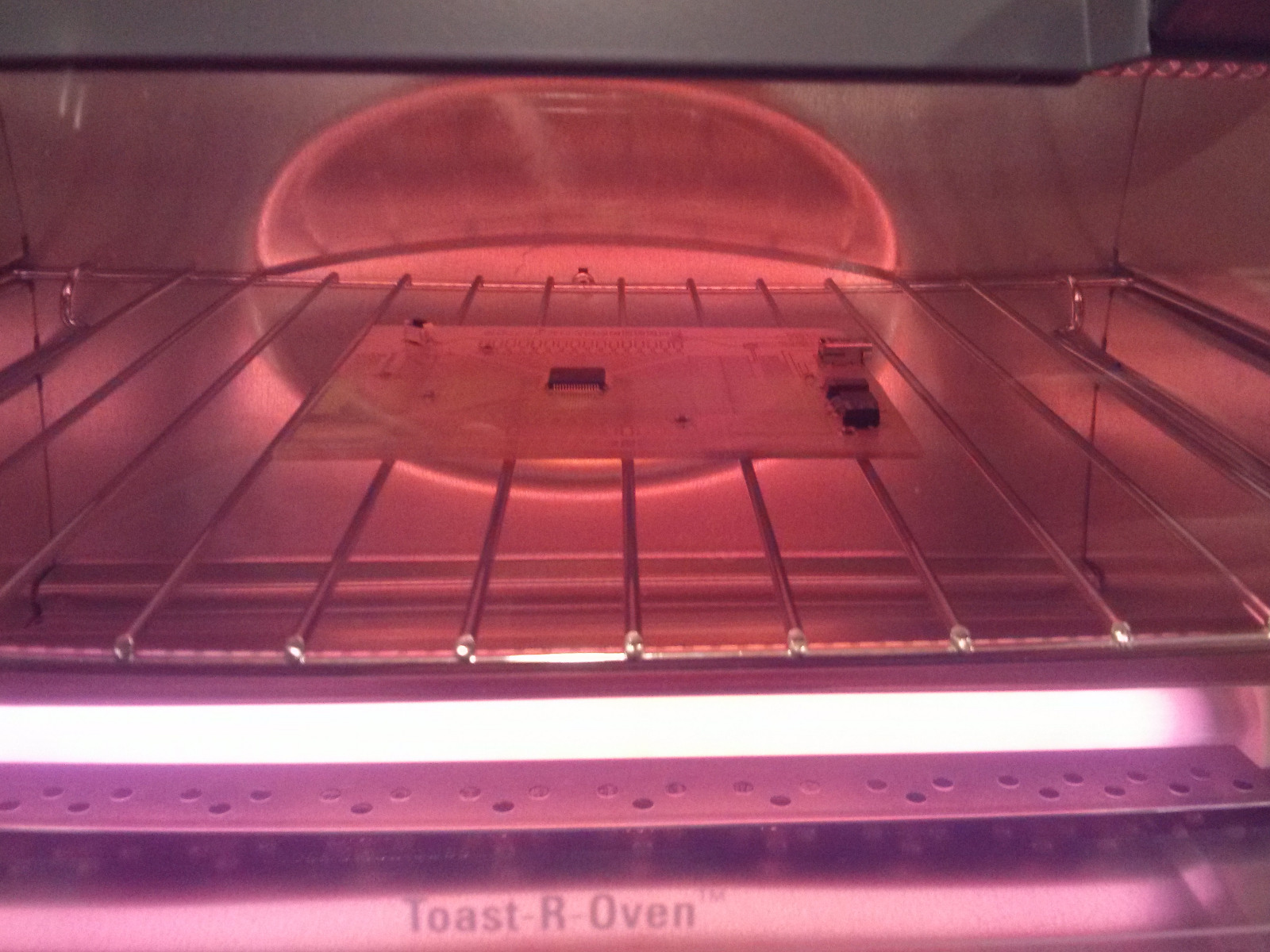
Step 10: Bake until the solder melts.
Step 11: Hand-solder the pin headers, then clean the board with some flux remover.
Now I have a board that can be placed on an electrically-conductive surface without fear. I think the four-way layout of pin headers will also make it easier to transition from a prototype to a custom PCB layout.